Alcatel
AMS 200 SE
The Alcatel AMS 200 SE is a Deep Reactive Ion Etching (DRIE) system for Silicon (Si) and Silicon-on-Insulator (SOI) wafers. The Alcatel AMS 200 SE uses an Inductively Coupled Plasma (ICP) source with RF power up to 3 kW and offers both RF and pulsed LF wafer biasing for flexible etching of dielectrics and silicon.[1]
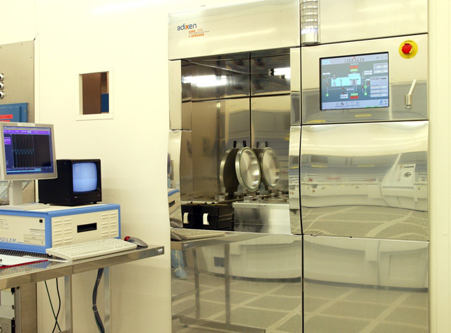
Power
3 kW at 13.56 MHz[1]
Vacuum
3 to 15 mbar[1]
Gas delivery
SF6 and C4F8 can be used in pulsed mode[1]
Optics
Laser interferometry at 670 nm[1]
What it is
The Alcatel AMS 200 SE is an optimized deep reactive ion etching system designed for silicon and silicon-on-insulator wafers.[1]
How it works
The system uses an electrostatic clamping chuck that is temperature controlled between minus ten and plus forty degrees Celsius. Wafer cooling is achieved by a helium film applied between the wafer backside and the chuck. The substrate holder height is adjustable between one hundred twenty and two hundred millimeters. The average ion energy is controlled by the substrate holder voltage biasing. Two biasing modes are available: pulsed low-frequency biasing with a maximum of six hundred watts, and RF biasing at 13.56 MHz with a maximum of five hundred watts. The system automatically selects the correct biasing mode based on the recipe.[1]
Where it fits in the process flow
The Alcatel AMS 200 SE supports three families of processes: silicon etching with a pulsed process, silicon etching with a continuous process, and dielectric etching. The pulsed process corresponds to the Bosch process for deep anisotropic etching. The system is used after lithographic patterning of a mask layer and before mask removal and cleaning steps.[1]
Applications
General reference — not yet source-verifiedDeep reactive ion etching systems are commonly applied in the fabrication of microelectromechanical systems, microfluidic devices, through-silicon vias, and other semiconductor and micro-optical components that require deep, vertical sidewalls and high aspect ratios.
- Silicon etching
- Silicon-on-insulator etching
- Dielectric etching
- Isotropic silicon release etching
Why won't it start?
Documented failure modes, common issues, and field considerations.
- The equipment is not microelectronic compatible.
- Borosilicate (Pyrex) and sodalime (floatglass) wafers can be loaded only with a backside conductive layer.
- For fused silica, Pyrex, and float glass wafers, a conductive backside layer is required because of the electrostatic clamping chuck.
What do the numbers mean?
Power & electrical11
- Wafer biasing modes
- RF (13.56 MHz) for dielectric etching and pulsed Low Frequency (LF) for silicon etching[1]
- Plasma source type
- Inductively Coupled Plasma (ICP) with RF power at 13.56 MHz, maximum 3 kW[1]
- Wafer biasing
- RF (13.56 MHz) for dielectric etching and pulsed low frequency for Si etching[1]
Vacuum & pumping11
Wafer handling11
- Wafer cooling / clamping
- Electrostatic Clamping Chuck (ESC) controlled in temperature for wafer cooling[1]
Gas & chemistry11
Optics & imaging4
Control & software1
Configuration & options6
Vintage & configurations
Documented models & variants
| Designation | Generation | Vintage | Changes | Source |
|---|---|---|---|---|
| AMS200 | — | — | Referenced as the AMS200 system and described as the same equipment in the source text. | epfl.ch[1] |
What replaced it?
Related models
- siblingSTS Multiplex ICP— Listed in the same etching equipment section.source[1]
- siblingSPTS Rapier— Listed in the same etching equipment section.source[1]
- siblingSPTS Synapse— Listed in the same etching equipment section.source[1]
- siblingSPTS APS— Listed in the same etching equipment section.source[1]
What does it need to run?
Site utility requirements, footprint, and infrastructure needed to install and operate this tool. Sourced from public records.
- Maximum ICP RF power3 kW at 13.56 MHz[1]
- He backside pressure range3 to 15 mbar[1]
- Wafer biasing modesRF (13.56 MHz) for dielectric etching and pulsed Low Frequency (LF) for silicon etching[1]
- Maximum substrate holder bias power600 W pulsed LF or 500 W RF[1]
- PumpingAdixen 1600 l/s turbo pump plus Adixen ADP122 rough pump[1]
- Gas lines7 mass flow controllers and 6 gases: SF6, C4F8, CH4, O2, Ar, He[1]
- Bosch process gasesSF6 and C4F8 can be used in pulsed mode[1]
- Plasma source typeInductively Coupled Plasma (ICP) with RF power at 13.56 MHz, maximum 3 kW[1]
- Backside helium pressure range3 to 15 mbar[1]
- Wafer biasing optionsPulsed LF (600 W max) or RF at 13.56 MHz (500 W max)[1]
- Pump systemAdixen 1600 l/s turbo pump + Adixen ADP122 rough pump; base pressure few 10^-7 mbar[1]
- Available gases and MFCsSF6 (0-1000 sccm), C4F8 (0-400 sccm and 0-100 sccm), CH4, O2, Ar, He; 7 MFCs total[1]
- RF power13.56 MHz, 3 kW maximum[1]
- Wafer biasing (RF)13.56 MHz, 500 W maximum[1]
- Helium backside pressure3 to 15 mbar[1]
- Turbo pumpAdixen 1600 l/s[1]
- Rough pumpAdixen ADP122[1]
- Base pressurefew 10⁻⁷ mbar[1]
- Number of mass flow controllers7 MFC for 6 gases[1]
- Gas flow SF₆0–1000 sccm (fast MFC)[1]
- Gas flow C₄F₈0–400 sccm (fast MFC) and 0–100 sccm[1]
- Gas flow CH₄0–100 sccm[1]
- Gas flow O₂0–100 sccm[1]
- Gas flow Ar0–200 sccm[1]
- Gas flow He0–200 sccm[1]
- Plasma sourceInductively Coupled Plasma (ICP) with RF 13.56 MHz, 3 kW maximum[1]
- Wafer biasingRF (13.56 MHz, 500 W max) or pulsed low-frequency (LF, 600 W max)[1]
- ESC cooling methodHelium backside film, pressure 3–15 mb[1]
- Pumping systemAdixen 1600 l/s turbo pump + Adixen ADP122 rough pump, base pressure few×10⁻⁷ mb[1]
- Gas lines7 mass flow controllers for 6 gases: SF₆ (0–1000 sccm, fast), C₄F₈ (0–400 sccm fast, 0–100 sccm), CH₄, O₂, Ar, He (all 0–200 sccm except noted)[1]
- Maximum RF power on ICP3 kW[1]
- Wafer biasingRF (13.56 MHz) for dielectric etching and pulsed low frequency for Si etching[1]
- He backside pressure3 to 15 mbar[1]
Where are the manuals?
Generated from public-source data on file. Enter your email to access — nothing is published; details are routed privately.
Not publicly documented
Field notes
No research found yet — worked with this tool? Share what you know.
Frequently asked questions
What is the maximum RF power for the ICP source?
The maximum RF power for the ICP source is 3 kW at 13.56 MHz.[1]
What is the pumping speed of the turbo pump?
The turbo pump has a pumping speed of 1600 liters per second.[1]
What is the temperature range of the substrate holder?
The substrate holder temperature can be adjusted between -10 °C and +40 °C.[1]
How is end point detection performed?
End point detection is performed by laser interferometry at a wavelength of 670 nm.[1]
Not publicly documented
The following facts about the AMS 200 SE are absent from this record as of this revision. First-hand knowledge or a citation closes a gap; every submission is reviewed before publication.
No publicly documented production dates or lifecycle milestones (introduction, end of production, EOL) for the AMS 200 SE are on record.
Answerable by: OEM historical records or a trade-press announcement
The control-system platform and OS era of the AMS 200 SE are not on record.
Answerable by: an engineer who operated it or OEM installation records
The process node or technology generation of the AMS 200 SE is not on record.
Answerable by: an OEM datasheet or a fab qualification report
No publicly documented compatible parts, consumables, or accessories for the AMS 200 SE are on record.
Answerable by: an OEM parts catalog or a service engineer
No publicly hosted manuals, SOPs, or datasheets for the AMS 200 SE are on record.
Answerable by: university cleanroom staff or an OEM application specialist
Sources & citations
Sources (1)Every fact above is drawn from these public sources
- [1]epfl.ch — epfl.chepfl.ch
Last updated Oct 8, 2026.
Compare with similar tools
View all →The Applied Materials 0010-47763 is an electrostatic chuck (ESC) assembly used in semiconductor etching processes.
The Applied Materials 0010-16392 is an electrostatic chuck assembly designed for 300 mm wafer processing, featuring a dual electrode configuration.
Oxford Instruments 100 ICP Fluorine is an inductively coupled plasma etcher for fluorine-based etching, supporting cryo DRIE and multiple etch gases including SF6 and C4F8.
