ASML
TWINSCAN NXE:3600D
Provisional entry — research in progress
This page was generated automatically from cited public sources and hasn't completed the full research pass yet. Every specification shown carries its source; more detail is added as research completes.
Node / era
5 nm, 3 nm
Optics
13.5 nm[1]
How it works
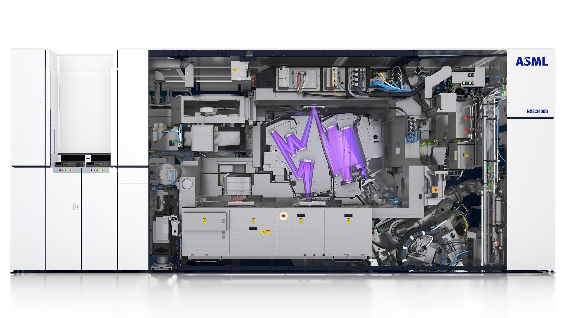
EUV lithography systems use extreme ultraviolet light with a wavelength of 13.5 nm to print microchips. The NXE:3600D uses a CO2 laser that fires two separate laser pulses at a fast-moving drop of tin to generate EUV light, doing so up to 50,000 times per second.[1]
EUV systems use several multilayer mirrors instead of lenses to guide the EUV light to the wafer, shrinking the reticle pattern by a factor of four. The entire light path and everything the light interacts with, from source to wafer, must be in a high vacuum because EUV light is absorbed by everything, including air.[1]
The NXE:3600D is a dual-stage system, meaning it has two wafer stages. One stage positions the wafer to within a quarter of a nanometer for each exposure, checking and adjusting 20,000 times per second. Precision robot arms transfer wafers in and out of the system's vacuum environment through an air lock, operating within a positioning accuracy of 25 µm and a uniform surface temperature within 2 mK.[1]
Where it fits in the process flow
The TWINSCAN NXE:3600D is used to print the most intricate layers on a chip, with the rest of the layers printed using various DUV systems. Both types of technology are required in parallel for many years to come.[1]
Chipmakers use NXE systems to print the highly complex foundation layers of their 7 nm, 5 nm and 3 nm nodes. The NXE:3600D specifically supports EUV volume production at the 5 and 3 nm Logic nodes and leading-edge DRAM nodes.[1]
Applications
Chips made with EUV lithography are enabling smart technology (cars, phones, and homes), augmented reality, artificial intelligence, and other applications. EUV lithography makes scaling more affordable for chipmakers and allows the semiconductor industry to continue its pursuit of Moore's Law.[1]
- 5 nm Logic nodes
- 3 nm Logic nodes
- Leading-edge DRAM nodes
What do the numbers mean?
Optics & imaging3
What replaced it?
Related models
- siblingASML TWINSCAN NXE:3800E— Also part of the NXE series, supports 2 nm Logic nodes and leading-edge DRAM nodessource[1]
Where are the manuals?
Generated from public-source data on file. Enter your email to access — nothing is published; details are routed privately.
Not publicly documented
Field notes
No research found yet — worked with this tool? Share what you know.
Not publicly documented
The following facts about the TWINSCAN NXE:3600D are absent from this record as of this revision. First-hand knowledge or a citation closes a gap; every submission is reviewed before publication.
No publicly documented production dates or lifecycle milestones (introduction, end of production, EOL) for the TWINSCAN NXE:3600D are on record.
Answerable by: OEM historical records or a trade-press announcement
No publicly documented variants, configuration options, or revision breakpoints of the TWINSCAN NXE:3600D are on record.
Answerable by: an OEM product catalog or an engineer who ordered or specified the tool
The control-system platform and OS era of the TWINSCAN NXE:3600D are not on record.
Answerable by: an engineer who operated it or OEM installation records
No publicly documented failure modes or field errata for the TWINSCAN NXE:3600D are on record.
Answerable by: a field service engineer, process engineer, or maintenance technician
No publicly documented compatible parts, consumables, or accessories for the TWINSCAN NXE:3600D are on record.
Answerable by: an OEM parts catalog or a service engineer
No research found yet — worked with this tool? Share what you know.
Sources & citations
Sources (1)Every fact above is drawn from these public sources
- [1]asml.com — asml.comasml.com
Last updated Sep 22, 2026.
Compare with similar tools
View all →Brooks 017-0146-01 is a prealigner manufactured by Brooks.
The EVG 101 is an advanced resist processing system for spin or spray coating and developing of wafers up to 300 mm.
